- 您现在的位置:买卖IC网 > Sheet目录317 > C8051F380-TB (Silicon Laboratories Inc)DEV KIT FOR C8051F38X
�� �
�
�C8051F380/1/2/3/4/5/6/7/C�
�22.1.� Supporting� Documents�
�It� is� assumed� the� reader� is� familiar� with� or� has� access� to� the� following� supporting� documents:�
�?�
�?�
�?�
�The� I� 2� C-Bus� and� How� to� Use� It� (including� specifications),� Philips� Semiconductor.�
�The� I� 2� C-Bus� Specification—Version� 2.0,� Philips� Semiconductor.�
�System� Management� Bus� Specification—Version� 1.1,� SBS� Implementers� Forum.�
�22.2.� SMBus� Configuration�
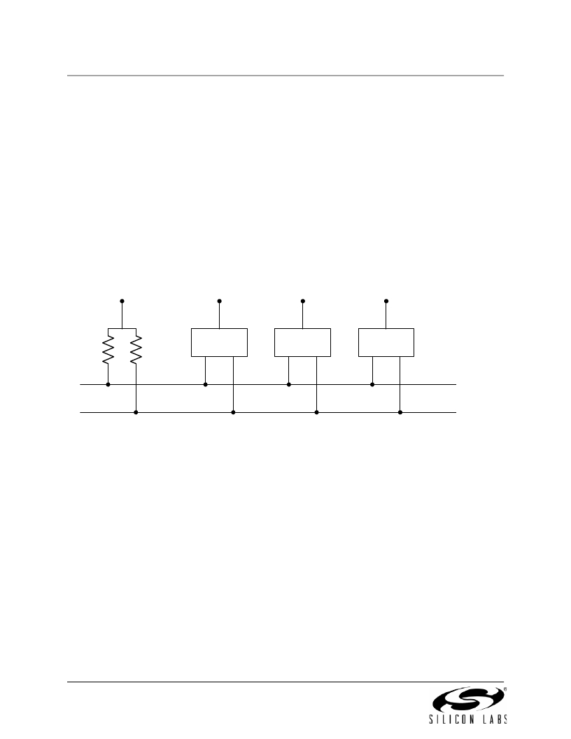
�Figure� 22.2� shows� a� typical� SMBus� configuration.� The� SMBus� specification� allows� any� recessive� voltage�
�between� 3.0� V� and� 5.0� V;� different� devices� on� the� bus� may� operate� at� different� voltage� levels.� The� bi-direc-�
�tional� SCL� (serial� clock)� and� SDA� (serial� data)� lines� must� be� connected� to� a� positive� power� supply� voltage�
�through� a� pullup� resistor� or� similar� circuit.� Every� device� connected� to� the� bus� must� have� an� open-drain� or�
�open-collector� output� for� both� the� SCL� and� SDA� lines,� so� that� both� are� pulled� high� (recessive� state)� when�
�the� bus� is� free.� The� maximum� number� of� devices� on� the� bus� is� limited� only� by� the� requirement� that� the� rise�
�and� fall� times� on� the� bus� not� exceed� 300� ns� and� 1000� ns,� respectively.�
�VDD� =� 5V�
�VDD� =� 3V�
�Master�
�Device�
�VDD� =� 5V�
�Slave�
�Device� 1�
�VDD� =� 3V�
�Slave�
�Device� 2�
�SDA�
�SCL�
�Figure� 22.2.� Typical� SMBus� Configuration�
�22.3.� SMBus� Operation�
�Two� types� of� data� transfers� are� possible:� data� transfers� from� a� master� transmitter� to� an� addressed� slave�
�receiver� (WRITE),� and� data� transfers� from� an� addressed� slave� transmitter� to� a� master� receiver� (READ).�
�The� master� device� initiates� both� types� of� data� transfers� and� provides� the� serial� clock� pulses� on� SCL.� The�
�SMBus� interface� may� operate� as� a� master� or� a� slave,� and� multiple� master� devices� on� the� same� bus� are�
�supported.� If� two� or� more� masters� attempt� to� initiate� a� data� transfer� simultaneously,� an� arbitration� scheme�
�is� employed� with� a� single� master� always� winning� the� arbitration.� It� is� not� necessary� to� specify� one� device�
�as� the� Master� in� a� system;� any� device� who� transmits� a� START� and� a� slave� address� becomes� the� master�
�for� the� duration� of� that� transfer.�
�A� typical� SMBus� transaction� consists� of� a� START� condition� followed� by� an� address� byte� (Bits7–1:� 7-bit�
�slave� address;� Bit0:� R/W� direction� bit),� one� or� more� bytes� of� data,� and� a� STOP� condition.� Bytes� that� are�
�received� (by� a� master� or� slave)� are� acknowledged� (ACK)� with� a� low� SDA� during� a� high� SCL� (see�
�Figure� 22.3).� If� the� receiving� device� does� not� ACK,� the� transmitting� device� will� read� a� NACK� (not� acknowl-�
�edge),� which� is� a� high� SDA� during� a� high� SCL.�
�The� direction� bit� (R/W)� occupies� the� least-significant� bit� position� of� the� address� byte.� The� direction� bit� is� set�
�to� logic� 1� to� indicate� a� "READ"� operation� and� cleared� to� logic� 0� to� indicate� a� "WRITE"� operation.�
�206�
�Rev.� 1.4�
�发布紧急采购,3分钟左右您将得到回复。
相关PDF资料
C8051F912DK
KIT DEV FOR C8051F91X/C8051F90X
C8051F930-TB
BOARD TARGET/PROTO W/C8051F930
C8051T610DB24
DAUGHTER BOARD T610 24QFN SOCKET
C8051T630DB20
BOARD SOCKET DAUGHTER 20-QFN
CAN-100
BOARD EVAL RS232 100QFP
CANADAPT28
KIT ADAPTER CANDEMOBOARD 28PLCC
CAT24AA01WI-GT3
IC EEPROM SERIAL 1KB I2C 8SOIC
CAT24AA02WI-G
IC EEPROM SERIAL 2KB I2C 8SOIC
相关代理商/技术参数
C8051F381
制造商:SILABS 制造商全称:SILABS 功能描述:USB DRIVER CUSTOMIZATION
C8051F381-GM
功能描述:8位微控制器 -MCU USB-64K-Flash
RoHS:否 制造商:Silicon Labs 核心:8051 处理器系列:C8051F39x 数据总线宽度:8 bit 最大时钟频率:50 MHz 程序存储器大小:16 KB 数据 RAM 大小:1 KB 片上 ADC:Yes 工作电源电压:1.8 V to 3.6 V 工作温度范围:- 40 C to + 105 C 封装 / 箱体:QFN-20 安装风格:SMD/SMT
C8051F381-GMR
功能描述:8位微控制器 -MCU USB-Flash-64k-ADC RoHS:否 制造商:Silicon Labs 核心:8051 处理器系列:C8051F39x 数据总线宽度:8 bit 最大时钟频率:50 MHz 程序存储器大小:16 KB 数据 RAM 大小:1 KB 片上 ADC:Yes 工作电源电压:1.8 V to 3.6 V 工作温度范围:- 40 C to + 105 C 封装 / 箱体:QFN-20 安装风格:SMD/SMT
C8051F381-GQ
功能描述:8位微控制器 -MCU USB-64K-Flash
RoHS:否 制造商:Silicon Labs 核心:8051 处理器系列:C8051F39x 数据总线宽度:8 bit 最大时钟频率:50 MHz 程序存储器大小:16 KB 数据 RAM 大小:1 KB 片上 ADC:Yes 工作电源电压:1.8 V to 3.6 V 工作温度范围:- 40 C to + 105 C 封装 / 箱体:QFN-20 安装风格:SMD/SMT
C8051F381-GQR
功能描述:8位微控制器 -MCU USB-Flash-64k-ADC RoHS:否 制造商:Silicon Labs 核心:8051 处理器系列:C8051F39x 数据总线宽度:8 bit 最大时钟频率:50 MHz 程序存储器大小:16 KB 数据 RAM 大小:1 KB 片上 ADC:Yes 工作电源电压:1.8 V to 3.6 V 工作温度范围:- 40 C to + 105 C 封装 / 箱体:QFN-20 安装风格:SMD/SMT
C8051F382
制造商:SILABS 制造商全称:SILABS 功能描述:USB DRIVER CUSTOMIZATION
C8051F382-GQ
功能描述:8位微控制器 -MCU USB-Flash-32k-ADC
RoHS:否 制造商:Silicon Labs 核心:8051 处理器系列:C8051F39x 数据总线宽度:8 bit 最大时钟频率:50 MHz 程序存储器大小:16 KB 数据 RAM 大小:1 KB 片上 ADC:Yes 工作电源电压:1.8 V to 3.6 V 工作温度范围:- 40 C to + 105 C 封装 / 箱体:QFN-20 安装风格:SMD/SMT
C8051F382-GQR
功能描述:8位微控制器 -MCU USB-Flash-32k-ADC RoHS:否 制造商:Silicon Labs 核心:8051 处理器系列:C8051F39x 数据总线宽度:8 bit 最大时钟频率:50 MHz 程序存储器大小:16 KB 数据 RAM 大小:1 KB 片上 ADC:Yes 工作电源电压:1.8 V to 3.6 V 工作温度范围:- 40 C to + 105 C 封装 / 箱体:QFN-20 安装风格:SMD/SMT